 ·
·
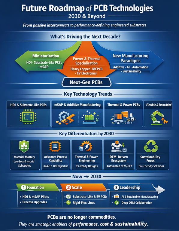
Executive summary
Printed Circuit Boards are evolving from passive interconnects into engineered substrates that shape system performance, cost and sustainability. Over the next decade we’ll see three converging forces drive the roadmap: extreme miniaturization (HDI & substrate-like PCBs), power/thermal specialization (heavy-copper, MCPCB, thermal substrates), and new manufacturing paradigms (mSAP, additive/3D printing, AI/automation) — all against a backdrop of sustainability and regional supply-chain reshoring. These changes create clear technical differentiators for companies that invest early in materials, process capability, and design-for-manufacturing pipelines.
1. Key technology trends (what to watch)
1.1 High-Density Interconnects (HDI) and Substrate-Like PCBs
- HDI will keep enabling smaller, multi-function modules (smartphones, wearables, medical implants) with finer lines, microvias and buried/staggered via stacks.
- Substrate-Like PCBs (SLP) — ultra-thin cores plus mSAP processes — are bridging PCBs and IC substrates, enabling multi-layer, fine-pitch routing for RF front ends and camera modules. This is a major enabler for compact mmWave/5G modules.
1.2 Modified Semi-Additive Processes (mSAP) & Additive Techniques
- mSAP allows trace geometries down to tens of microns and is critical for SLP/HDI.
- Additive manufacturing (including conductive inks and selective metallization) is maturing for prototyping and niche production; emerging work on recyclable, liquid-metal 3D PCBs shows longer-term potential for sustainable prototyping.
1.3 Thermal & Power-Handling PCBs (Heavy Copper, MCPCB)
- EV power electronics, battery management and fast chargers demand thick copper, specialized plating and hybrid substrates for heat spreading and current carrying capacity. Expect rapid growth here.
1.4 Flexible / Rigid-Flex & Embedded Components
- Flexible and rigid-flex boards become mainstream across wearables, automotive connectors and avionics. Embedding passives/actives reduces BOM and improves reliability for constrained form factors.
1.5 Automation, AI, Industry 4.0 in Manufacturing
- AI-driven DFM checks, computer vision for defect detection, predictive maintenance, and closed-loop process control will materially reduce yield losses and accelerate ramp times.
2. Technical strengths & differentiators (what wins customers)
- Material mastery — owning or qualifying low-loss laminates, ceramic substrates, heavy-copper stacks, and hybrid thermal substrates lets you serve high-frequency and power markets with measurable performance gains.
- Process depth (mSAP, laser, multi-layer HDI) — capability to produce substrate-like stacks, down to 20 μm lines, is an immediate differentiator for RF/optics/miniature camera modules.
- Thermal & power engineering — design rules and manufacturing know-how for thick copper, plated through-holes, thermal vias and metal cores unlock EV and power electronics markets.
- Design-for-manufacturing ecosystem — integrated DFM/DFT/automated layout checks that fold back into manufacturing cut time-to-market and defects.
- Sustainable offerings — recyclable prototyping, lower-chemistry processes, and material take-back programs will differentiate with eco-conscious OEMs.
3. Roadmap (practical timeline & priorities)
- Implement HDI and mSAP pilots; qualify low-loss laminates; upgrade process control and automated inspection.
- Invest in DFM/DFT tooling and close collaboration with key OEMs (5G modules, camera modules).
- Scale substrate-like PCB production, thick-copper capacity for EV suppliers, and rigid-flex lines for wearables/medical.
By Lakshmanan CT
Senior Manager, PCB Design
No comments yet. Login to start a new discussion Start a new discussion