Advanced PCB Design & Engineering
From concept to production — optimized layouts, signal integrity, and manufacturing-ready designs for reliable hardware products.
What We Deliver
End-to-end PCB engineering from schematic design to manufacturing, testing, and compliance certifications.
Our designers ensure performance, signal reliability, and mechanical integrity for complex electronics.
- High-speed & multi-layer PCB layouts
- DFM, DFA & EMC best practices
- Prototype, fabrication & assembly support
PCB Design Expertise
Schematic Design
- Component Selection
- NET Creation & BOM
- Design Validation
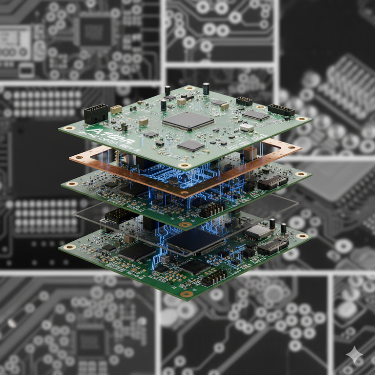
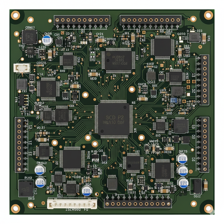
PCB Layout & Routing
- Multi-layer routing
- High-speed & RF design
- Thermal & mechanical integrity
Signal Integrity & Testing
- EMI/EMC Mitigation
- DFT, DFM & DFA
- Prototype Debugging
Fabrication Support
- Gerber & manufacturing outputs
- Vendor coordination
Assembly Engineering
- Pick & place support
- PCBA validation
Tools & Technology
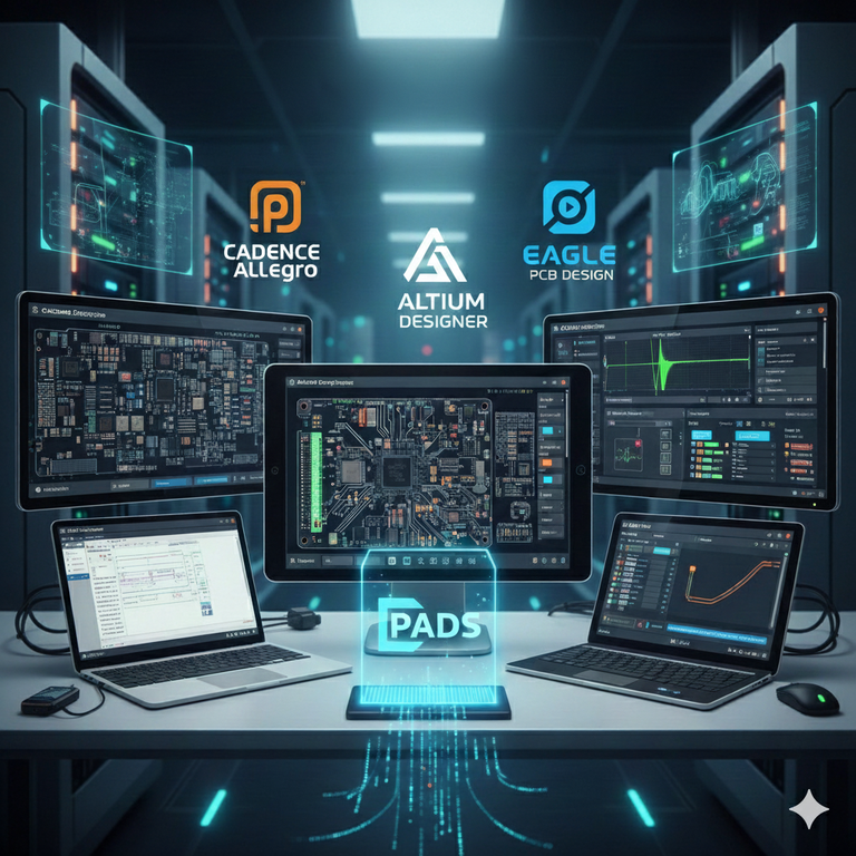
ECAD Tools
Altium · Cadence Allegro · KiCad · OrCAD
Proteus · Eagle · PADs

Compliance & Standards
RoHS · IPC · CE · FCC · UL